Working Of P-n Junction Diode Pdf

Working of p-n junction diode pdf
A diode (PN junction) in an electrical circuit allows current to flow more easily in one direction than another. Forward biasing means putting a voltage across a diode that allows current to flow easily, while reverse biasing means putting a voltage across a diode in the opposite direction.
What is PN junction explain Construction & working of PN junction?
A P-N Junction Diode is formed by doping one side of a piece of silicon with a P-type dopant (Boran) and the other side with a N-type dopant (phosphorus). Ge can be used instead of Silicon. The P-N junction diode is a two-terminal device. This is the basic construction of the P-N junction diode.
What is PN junction diode PDF?
A p-n junction is the metallurgical boundary between the n and p-regions of a semiconductor crystal. P-n junctions consist of two semiconductor regions of opposite type. Such junctions show a pronounced rectifying behavior. They are also called p-n diodes in analogy with vacuum diodes.
How PN junction diode works as a switch?
The PN junction, when forward biased acts as close circuited and when reverse biased acts as open circuited. Hence the change of forward and reverse biased states makes the diode work as a switch, the forward being ON and the reverse being OFF state.
What is pn junction diode explain its working in forward bias?
Forward bias or biasing is where the external voltage is delivered across the P-N junction diode. In a forward bias setup, the P-side of the diode is attached to the positive terminal and N-side is fixed to the negative side of the battery. Here, the applied voltage is opposite to the junction barrier potential.
What is pn junction explain working of PN junction diode in forward and reverse bias?
A P-N junction diode is said to be forward biased when the positive terminal of a cell or battery is connected to the p-side of the junction and the negative terminal to the n side. When diode is forward-biased the depletion region narrows and consequently, the potential barrier is lowered.
What is PN junction with diagram?
Definition: A P-N junction is an interface or a boundary between two semiconductor material types, namely the p-type and the n-type, inside a semiconductor. In a semiconductor, the P-N junction is created by the method of doping.
What is PN junction diode explain its construction and working with suitable diagram?
PN Junction diode is a device made of two semiconductor material joined together with the required amount of impurity. These materials are N-type, having electrons are majority carrier and P-type material, having holes are majority carrier. With proper biasing, PN diode allows current to flow in SINGLE DIRECTION.
What is application of PN junction diode?
Application of PN Junction Diode The junction which is the p-n junction diode can be used as a photodiode, the diode which is sensitive to the light when the configuration of the diode is reverse-biased. It can be used as a solar cell.
What is the symbol of pn junction?
PN Junction Diode Symbol The circuit symbol for a diode is an arrow and bar shown in Fig. 7.1. The arrowhead indicates the conventional direction of current flow when the diode is forward biased (i.e. from the positive terminal through the device to the negative terminal).
What are the properties of pn junction?
It can rectify electric current, inject minority carriers, create a potential barrier, make use of its capacitance properties, accumulate space charge, create various non-linear current—voltage characteristics, transform light energy into electrical, react to various kinds of irradiation, emit light radiation when a
How pn junction is formed?
P-n junctions are formed by joining n-type and p-type semiconductor materials, as shown below. Since the n-type region has a high electron concentration and the p-type a high hole concentration, electrons diffuse from the n-type side to the p-type side.
Why pn junction is called diode?
Why is p-n-junction is also called a junction diode ? Solution : A p-n-junction allows a large current to flow through it when forward biased and it offers a high resistance when reverse biased. The unidirectional property is similar to that of vacuum diode. Hence, p-n-junction is also called a junction diode.
Which is an example of pn junction diode?
Terminals of pn junction diode For example, bus terminal or terminus is a place at which all the buses begins or ends. Similarly, in a p-n junction diode, terminal refers a point at which charge carriers begins or ends. P-n junction diode consists of two terminals: positive and negative.
What is difference between forward and reverse bias?
In a standard diode, forward biasing occurs when the voltage across a diode permits the natural flow of current, whereas reverse biasing denotes a voltage across the diode in the opposite direction. However, the voltage present across a diode during reverse biasing does not produce any significant flow of current.
How does the P-N junction works under reverse bias?
In reverse bias a voltage is applied across the device such that the electric field at the junction increases. The higher electric field in the depletion region decreases the probability that carriers can diffuse from one side of the junction to the other, hence the diffusion current decreases.
What is forward bias and reverse bias with diagram?
| Basis for Comparison | Forward Biasing | Reverse Biasing |
|---|---|---|
| Barrier Potential | Reduces | Strengthen |
| Voltage | The voltage of an anode is greater than cathode. | The voltage of cathode is greater than an anode. |
| Forward Current | Large | Small |
| Depletion layer | Thin | Thick |
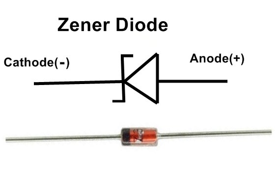
What are the types of P-N junction diode?
Diode is a PN junction device. ... Different types of PN-junction diodes
- Light Emitting Diode (LED)
- Photodiode. ...
- Solar Cell. ...
- Zener Diode.
Which diode is worked in reverse bias mode?
The Zener Diode is used in its “reverse bias”. Current starts to flow through the diode to limit this increase in voltage. Therefore the Zener diode will drain the current through it which is called a regulator.
What devices use pn junction?
p-n diodes are the basis for solar cells, photodiodes, light-emitting diodes (LEDs), and laser diodes. Solar cells are illuminated p-n junctions. They convert sunlight into electricity. Photodiodes are p-n junctions held in reverse bias used to detect light.
10 Working of p-n junction diode pdf Images
Semiconductor PN Junction Diode Working PN Diode VI Characteristics

Semiconductor PN Junction Diode Working PN diode VI characteristics

Characteristics and Working of PN Junction Diode Diode Circuits

Semiconductor PN Junction Diode Working PN diode VI characteristics

Diodes Explained The basics how diodes work working principle pn

The PN Junction Diode Animation Diode Junction Physical science
Semiconductor PN Junction Diode Working PN diode VI characteristics

Forming a pn junction Junction Christmas coloring pages Form

How a PN Junction Formed in a Diode
Post a Comment for "Working Of P-n Junction Diode Pdf"